

Boosting Light
to Transform Connectivity
Revolutionizing optical communication with Erbium-Doped Waveguide Amplifier (EDWA) technology offering compact, scalable, & high-performance on-chip gain.
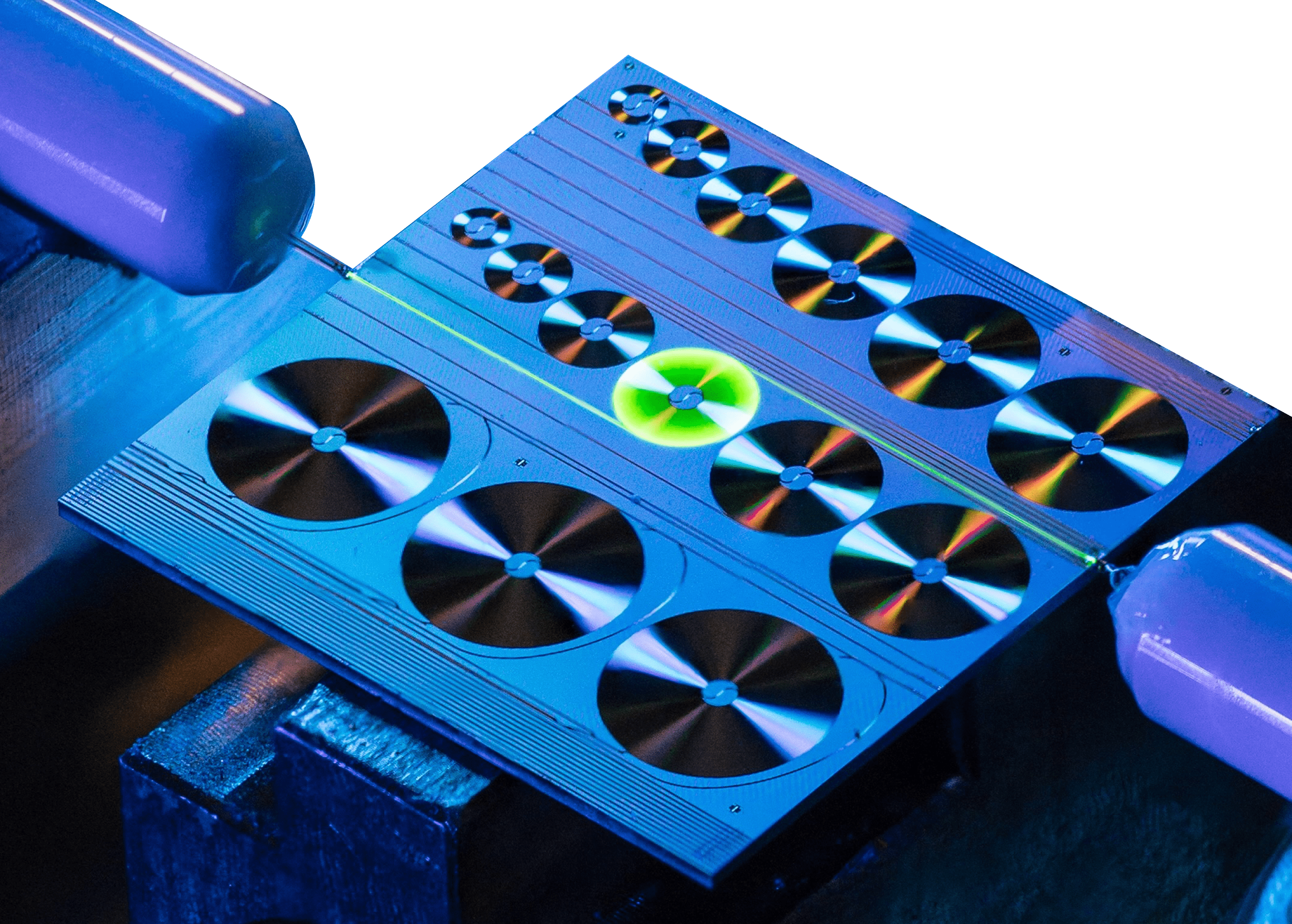
Leading the Future with Rare-Earth Ion-Doped Photonic Technology
EDWATEC is pioneering rare-earth ion-doped photonic technology to deliver unmatched performance, cost-efficiency, and scalability—powering the future of data, telecom, and AI.
High Performance
The device features 30 dB on-chip gain, 300 mW on-chip output power, a low noise figure (<5 dB), and temperature-insensitive gain.
Low Cost
Wafer-scale fabrication and flexible integration of passive and active photonic components enable cost-efficient, high-volume production.
Scalable
Monolithic integration with silicon photonics foundry process allowing large volume wafer scale fabrication.
Multi Lane
Integration of multiple amplifier lanes on a single photonic chip for massively parallel applications.
Compact
Ultra-compact, chip-scale amplifiers with mm² footprints.
Extended Range
Possibility to incorporate other ions to address a wide range of wavelengths.


Pioneering Rare-Earth Ion-Doped Photonic Circuits
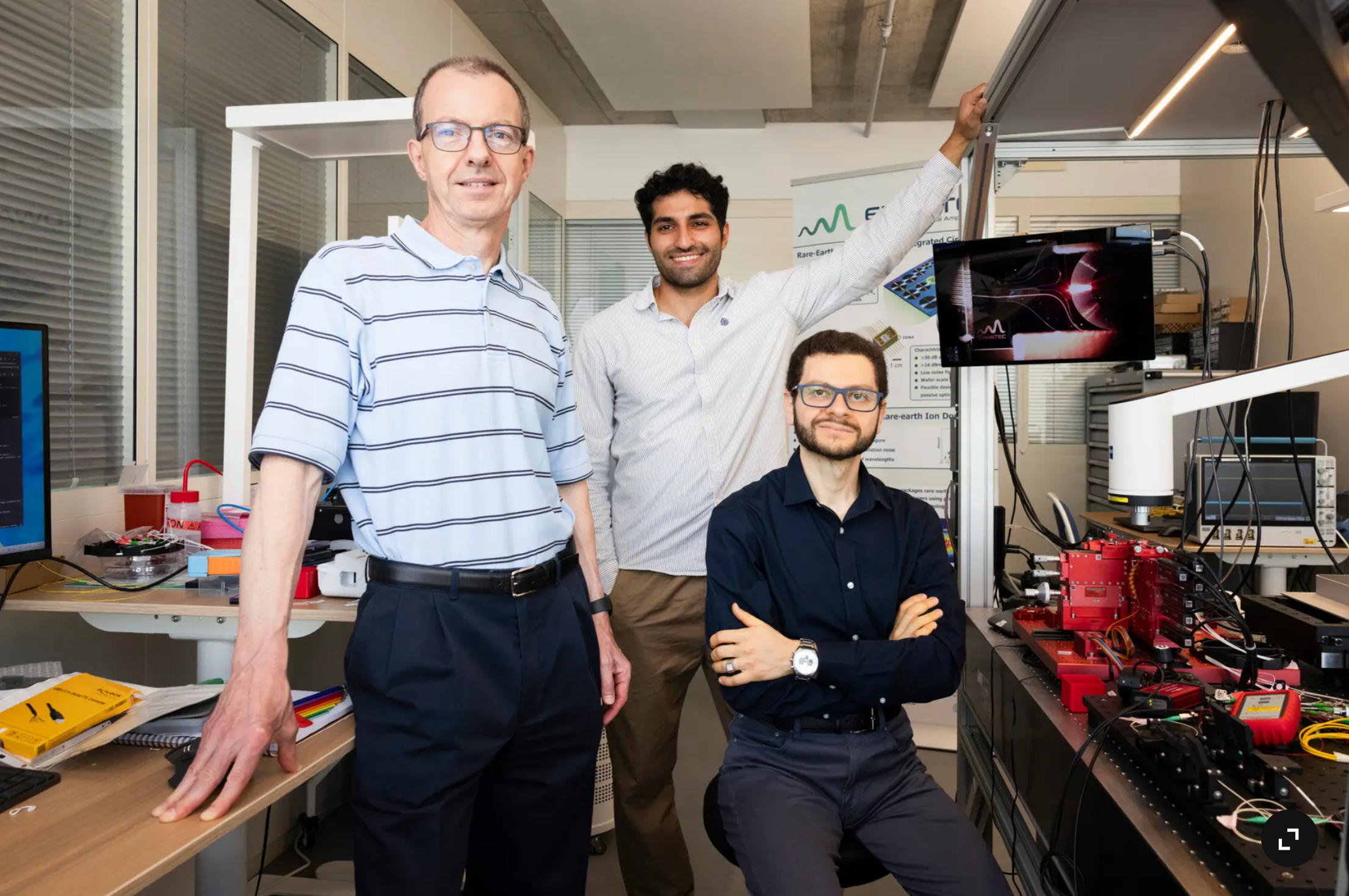
EDWATEC, a Swiss high-tech startup, manufactures rare-earth ion-doped photonic integrated circuits.
EDWATEC specializes in providing tailored solutions through its proprietary Er-doped PIC technology for compact, scalable, and high-performance optical amplifiers and lasers. Our distinct advantage lies in access to state-of-the-art nano-fabrication facilities combined with our team’s expertise in photonics design and measurement.
Latest Updates & Innovations

Interview with Alluvium Media at Deep Tech Momentum in Berlin
EDWATEC Co-founder and CTO Amir Youssefi speaks with Gareth Joseph from Alluvium Media at Deep Tech Momentum in Berlin about the role of on-chip optical amplification in future AI infrastructure and EDWATEC’s plans for rapid scale-up.
EDWATEC featured in 24 heures and Tribune de Genève
24 heures and Tribune de Genève feature EDWATEC in an in-depth article exploring how our integrated optical amplifiers can support the next generation of AI data centers and strengthen Switzerland’s role in the future AI market.

EDWATEC Wins the Grand Prize at the 2026 >>venture>> Startup Competition
EDWATEC has been awarded the Grand Prize of the 2026 >>venture>> Startup Competition, selected among more than 450 startups from across Switzerland.