
EDWA platform,
Engineered for Scale

Our Technology
EDWATEC’s erbium-doped photonic integrated circuits are based on low-loss silicon nitride waveguides doped via controlled ion implantation. This process ensures precise overlap between the optical mode and the active region of the waveguide, enabling efficient on-chip amplification with high gain, low noise, and minimal propagation loss. The architecture supports long interaction lengths within a compact footprint through optimized spiral geometries
By integrating rare-earth ions directly into the waveguide core, EDWATEC achieves stable population inversion and strong pump-signal conversion efficiency. The monolithic integration of EDWAs with silicon photonics offers tight control over doping profiles, and scalable wafer-level fabrication—delivering the core building block for high-performance optical amplification in integrated photonics.
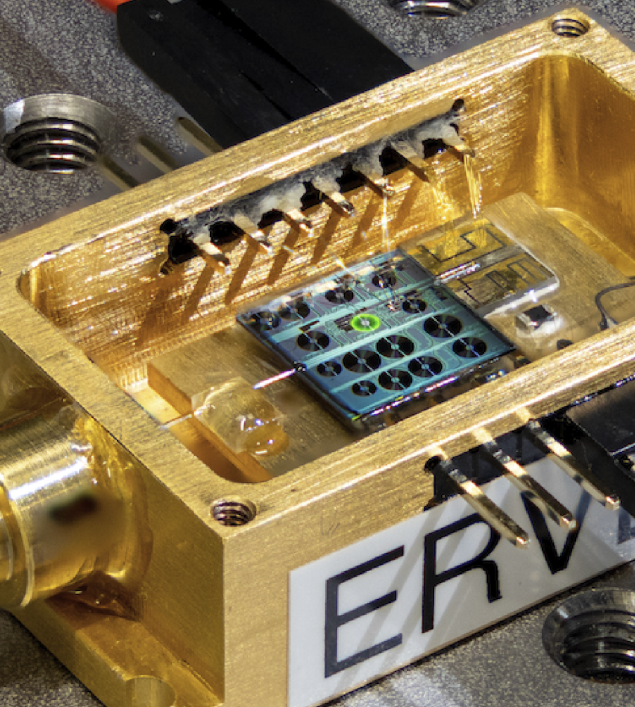
Custom Design & Fabrication
Custom design and fabrication enable precise, tailored solutions using 3D printing, CNC machining, and laser cutting. This approach boosts innovation, reduces waste, and ensures a perfect fit for any project.
Monolithic Integration with Silicon Photonics
Monolithic integration embeds photonic components on a single silicon chip, enabling compact, high-speed optical systems for data centers, telecom, and sensing.
Hybrid Integration with Photonic Products.
Hybrid integration combines different photonic materials and components to enhance performance and functionality. This approach enables more efficient, scalable, and versatile optical systems for applications in telecom, computing, and sensing.
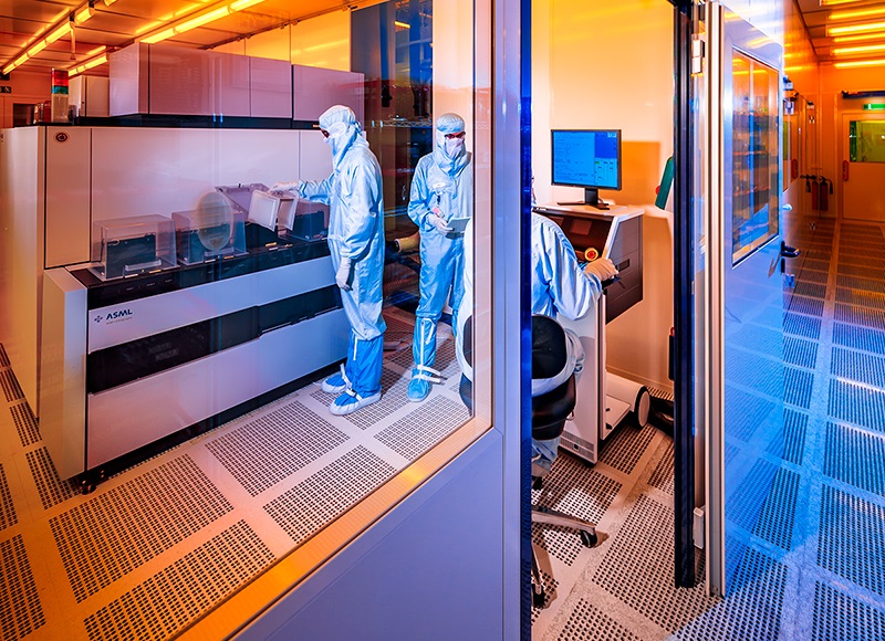
In-House Streamlined Design and Fabrication
At EDWATEC, the complete R&D cycle—including design, fabrication, and characterization—is performed in-house, enabling rapid development and iteration of integrated photonic devices. This streamlined approach reduces lead times, ensures tight control over process parameters, and accelerates the transition from concept to validated prototype. By combining nanofabrication capabilities with dedicated optical testing infrastructure, EDWATEC efficiently develops and refines erbium-doped photonic circuits with consistent performance and scalability.
EDWL: Erbium-Doped Waveguide Laser
EDWATEC’s erbium-doped waveguide lasers (EDWLs) leverage integrated erbium-doped spiral waveguides as external cavities to achieve ultra-narrow linewidths below 50 Hz and high spectral purity. These chip-scale lasers feature temperature-insensitive optical gain and low-loss cavity designs, ensuring exceptional frequency stability and minimal phase noise across a wide operational range. Engineered for full tunability across the C+L bands, EDWLs support precise wavelength control using thermo-optic tuning mechanisms. Their compact architecture enables integration with other photonic components on the same chip, offering a scalable solution for high-coherence applications such as coherent communication, sensing, and spectroscopy.